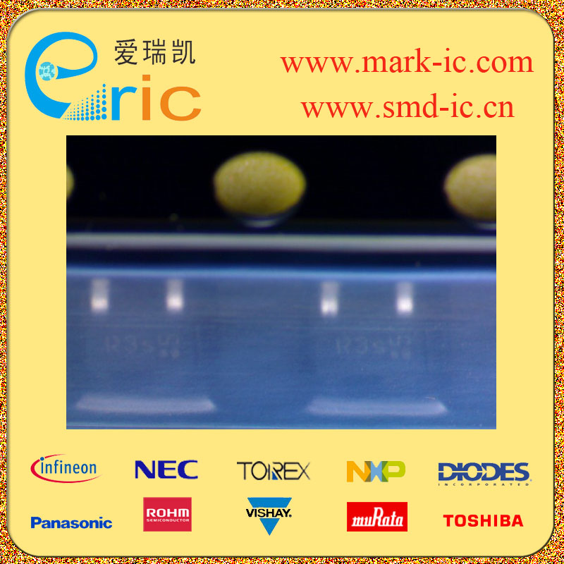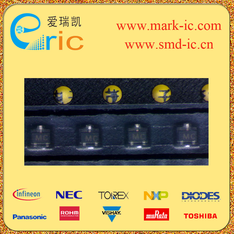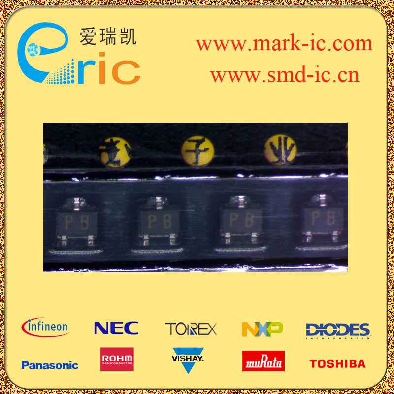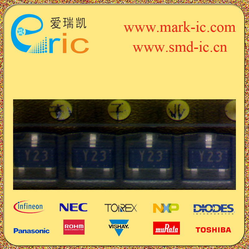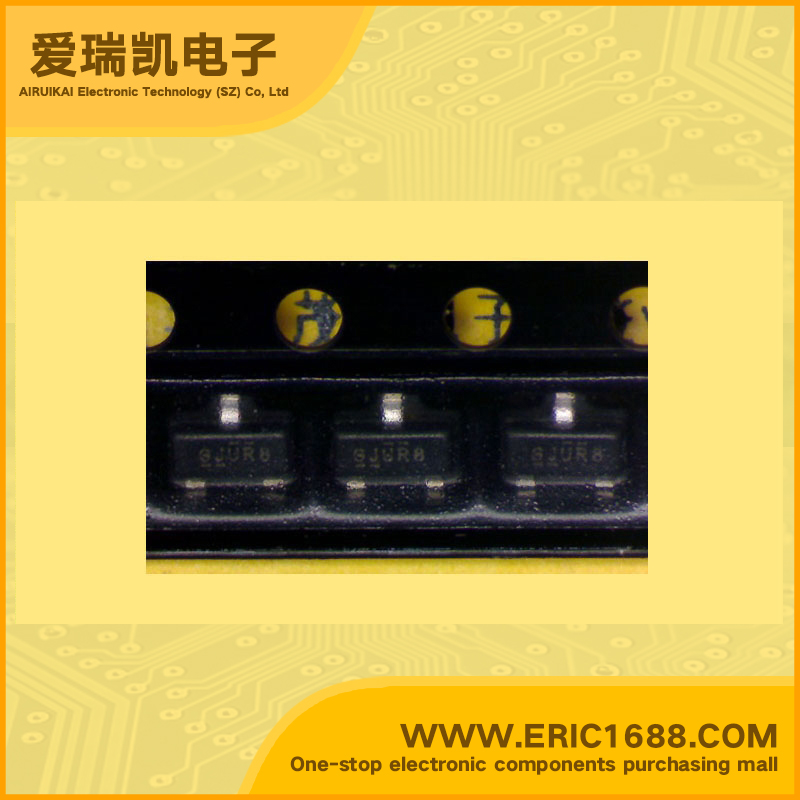
IRLML2502TR N沟道MOSFET 20V 4.2A SOT-23/SC-59 marking/标记 G
| 最大源漏极电压Vds Drain-Source Voltage | 20V |
| 最大栅源极电压Vgs(±) Gate-Source Voltage | |
| 最大漏极电流Id Drain Current | 4.2A |
| 源漏极导通电阻ΩRds DΩ/Ohmain-SouΩ/Ohmce On-State Ω/Ohmesistance | 0.045Ω/Ohm @4.3A,4.5V |
| 开启电压Vgs(th) Gate-Source Threshold Voltage | 0.60-1.2V |
| 耗散功率Pd Power Dissipation | 1.25W |
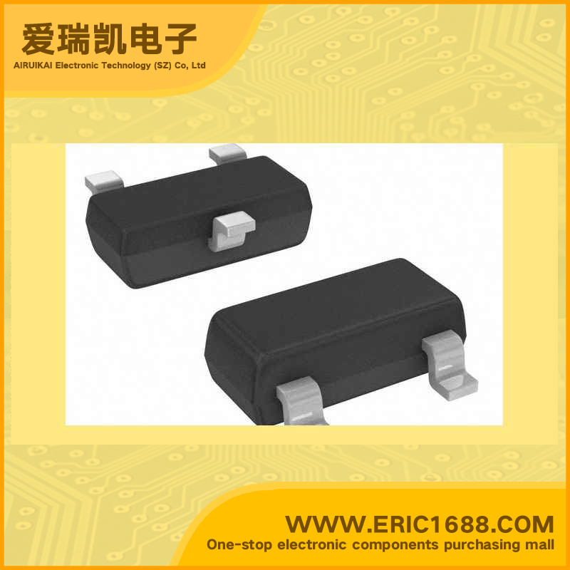
| Description & Applications | HEXFET Power MOSFET These N-Channel MOSFETs from International Rectifier utilize advanced processing techniques to achieve extremely low on-resistance per silicon area. This benefit, combined with the fast switching speed and ruggedized device design that HEXFET power MOSFETs are well known for, provides the designer with an extremely efficient and reliable device for use in battery and load management. A thermally enhanced large pad leadframe has been incorporated into the standard SOT-23 package to produce a HEXFET Power MOSFET with the industry's smallest footprint. This package, dubbed the Micro3, is ideal for applications where printed circuit board space is at a premium. The low profile (<1.1mm) of the Micro3 allows it to fit easily into extremely thin application environment such as portable electronics and PCMCIA cards. The thermal resistance and power dissipation are the best available. Ultra Low On-Resistance N-Channel MOSFET OT-23 Footprint Low Profile (<1.1mm) vailable in Tape and Reel Fast Switching |
| 描述与应用 | HEXFET 功率MOSFET 这些N沟道MOSFET的国际整流器 利用先进的加工技术,以实现极为 低导通电阻每硅片面积。这样做的好处,结合 开关速度快和坚固耐用的设备的设计 HEXFET功率MOSFET是众所周知的,提供 设计师使用电池和负载管理的一个非常有效和可靠的设备。增强型散热一直大焊盘引线框架 纳入标准SOT-23封装,以产生一种HEXFET功率MOSFET,具有业界最小的足迹。这个包,冠以的MICRO3,是理想的应用印刷电路板空间是一个溢价。扁平(高度<1.1mm)的MICRO3允许它很容易融入极薄的应用环境,如便携式电子设备和PCMCIA卡。热电阻和功耗是最好的。 超低导通电阻 N沟道MOSFET SOT-23的脚印 薄型(高度<1.1mm) 可在磁带和卷轴 快速切换 |
| 规格书PDF |