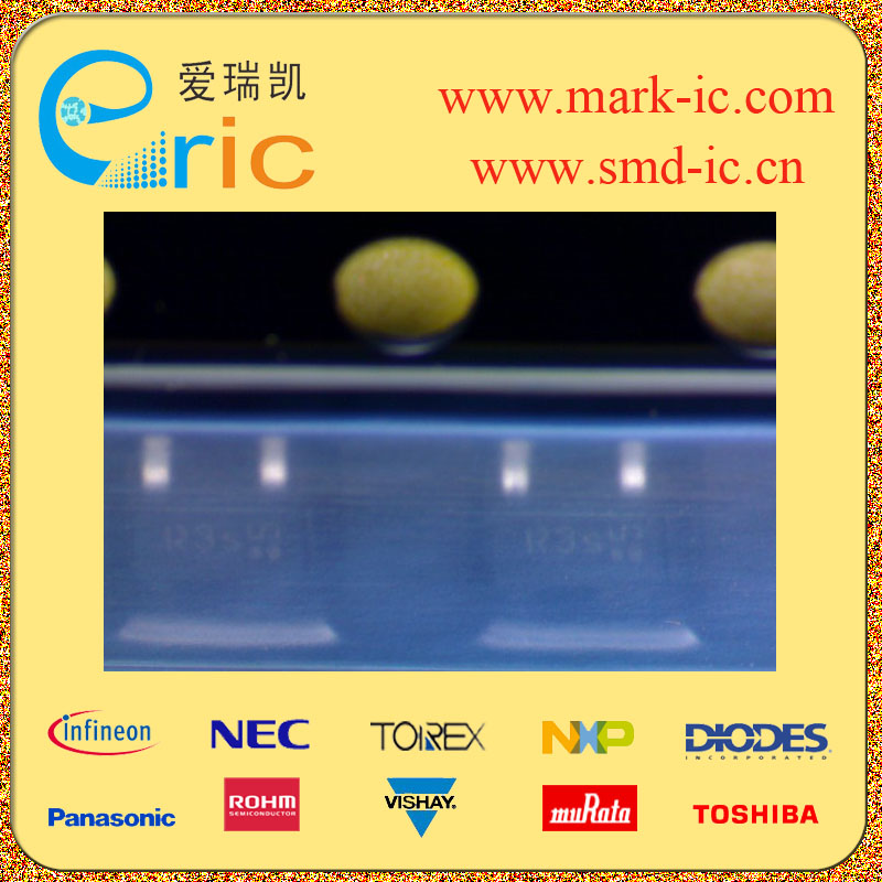
D触发器 HD74LV2G74AUSE SSOP8 标记 L74
| 逻辑类型Logic Type | 设置(预设)和复位 Set(Preset) and Reset |
| 电路数Number of Circuits | D型 D-Type |
| 输入数Number of Inputs | 差分 Differential |
| 电源电压VccVoltage - Supply | 1 |
| 静态电流IqCurrent - Quiescent (Max) | 1 |
| 输出高,低电平电流Current - Output High, Low | 20MHz |
| 低逻辑电平Logic Level - Low | 1ns |
| 高逻辑电平Logic Level - High | 正边沿 Positive Edge |
| 传播延迟时间@Vcc,CLMax Propagation Delay @ V, Max CL | 12mA,12MA |
| Description & Applications | -0.5-7.0V |
| 描述与应用 | Single D–type Flip Flops with Preset and Clear Description The HD74LV2GT74A has independent data, preset, clear, and clock inputs Q and Q outputs in an 8 pin package. The input data is transferred to the output at the rising edge of clock pulse CLK. The input protection circuitry on this device allows over voltage tolerance on the input, allowing the device to be used as a logic–level translator from 3.0 V CMOS Logic to 5.0 V CMOS Logic or from 1.8 V CMOS logic to 3.0 V CMOS Logic while operating at the high-voltage power supply. Low voltage and high-speed operation is suitable for the battery powered products (e.g., notebook computers), and the low power consumption extends the battery life. Features • The basic gate function is lined up as Renesas uni logic series. • Supplied on emboss taping for high-speed automatic mounting. • TTL compatible input level. Supply voltage range : 3.0 to 5.5 V Operating temperature range : –40 to +85°C • Logic-level translate function 3.0 V CMOS logic → 5.0 V CMOS logic (@VCC = 5.0 V) 1.8 V or 2.5 V CMOS logic → 3.3 V CMOS logic (@VCC = 3.3 V) • All inputs VIH (Max.) = 5.5 V (@VCC = 0 V to 5.5 V) All outputs VO (Max.) = 5.5 V (@VCC = 0 V) • Output current ±6 mA (@VCC = 3.0 V to 3.6 V), ±12 mA (@VCC = 4.5 V to 5.5 V) • All the logical input has hysteresis voltage for the slow transition. • Ordering Information |
| 规格书PDF |