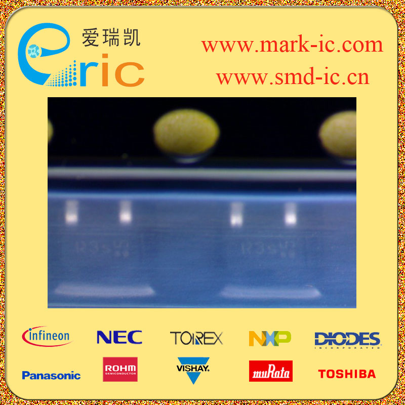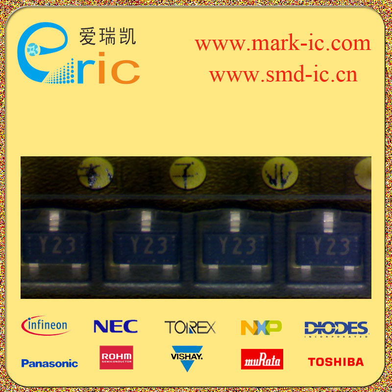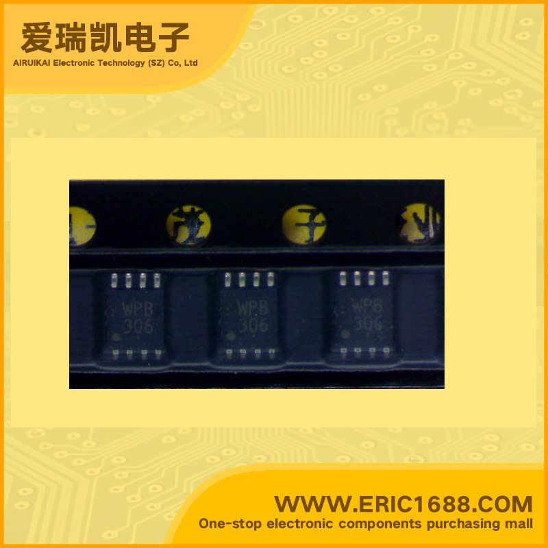
TC7WPB306FK 解码器、多路复用器、信号开关 VFSOP8/US8 标记WPB306
| 逻辑类型Logic Type | 总线开关 Bus Switch |
| 电路数Number of Circuits | |
| 输入数Number of Inputs | |
| 电源电压VccVoltage - Supply | |
| 静态电流IqCurrent - Quiescent (Max) | 双电源 Dual Supply |
| 输出高,低电平电流Current - Output High, Low | 1.65 V ~ 5 V 2.3 V ~ 5.5 V |
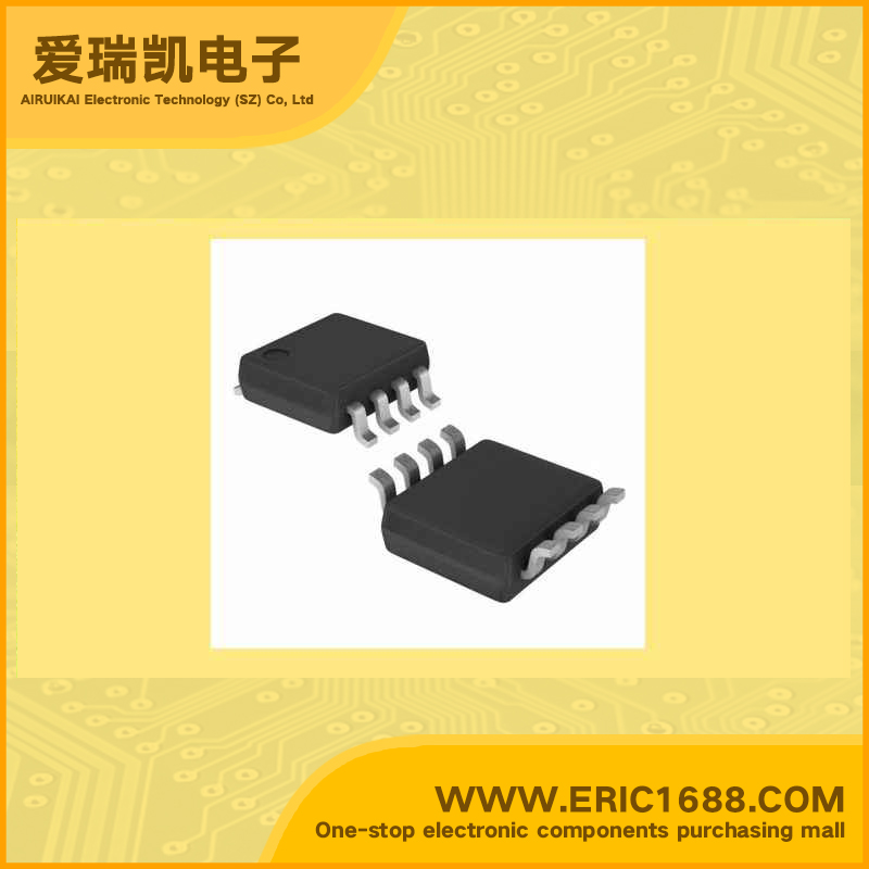
| 低逻辑电平Logic Level - Low | The TC7WPB306 and TC7WPB307 are high-speed CMOS two-bit bus switches with low ON-resistance that allow interfacing between different voltage nodes. These devices have two separate power supplies, VL for a 1.8-V, 2.5-V or 3.3-V bus and VH for a 2.5-V, 3.3-V or 5.0-V bus. For bidirectional level-shifting, the VH pin is connected to a high-voltage power supply through a bias resistor, and pull-up resistors are connected between the high-voltage power supply and the switch. The enable signal can be used to disable the device so that the buses are effectively isolated. For the TC7WPB306, Output Enable (OE) is active-High: When OE is High, the switch is on; when Low, the switch is off. For the TC7WPB307, Output Enable ( OE ) is active-Low: When OE is Low, the switch is on; when High, the switch is off. The TC7WP306 and TC7WP307 support power-down protection by incorporating 5.5-V-tolerant control inputs. The bus switch channels are fabricated with NMOS technology. All inputs are equipped with protection circuits against static discharge or transient excess voltage. Operating voltage: 1.8-V to 2.5-V, 1.8-V to 3.6-V, 1.8-V to 5.5-V, 2.3-V to 3.6-V, 2.3-V to 5.5-V or 3.0-V to 5.5-V bidirectional interface Operating voltage: VL = 1.65 to 5.0 V, VH = VL + 0.5 to 5.5 V High-speed operation: tpd = 0.12ns(max) (VL = 3.0 V, VH = 4.5 V) Low ON-resistance: RON = 3.0 Ω (typ.) (ON-resistance test circuit: VIS = 0 V, IIS = 30 mA, VH = 4.5 V) ESD performance: Machine model ≥ ±200 V Human body model ≥ ±2000 V 5.5-V tolerance and power-down protection at the Output Enable input. Packages: CSON8 (CST8), SSOP8 (US8) |
| 高逻辑电平Logic Level - High | TC7WPB306和TC7WPB307是高速CMOS 2位总线开关,具有低导通电阻,允许连接不同电压节点之间。这些器件具有两个独立的电源,VH:1.8 V,2.5 V或3.3 V总线,VL:2.5 V,3.3 V或5.0 V总线。对于双向电平移位,VH引脚通过一个偏置电阻连接到高电压电源供应器,上拉电阻器连接在高电压的电源和开关之间。使能信号可用于禁用设备使总线有效隔离。 对于TC7WPB306,输出使能(OE)有效高:当OE为高,开关是开着的,当低,开关处于关闭状态。对于TC7WPB307,输出使能(OE)低有效:当OE是低电平时,开关是开着的,是高时,开关处于关闭状态。TC7WP306和TC7WP307支持断电保护功能,结合5.5V容错控制输入。 总线开关通道NMOS技术制作。所有输入都配备了防静电放电保护电路或瞬态过电压。 工作电压:1.8 V到2.5 V,1.8 V至3.6 V,1.8 V至5.5 V,2.3 V至3.6 V,2.3 V到5.5 V或3.0 V到5.5 V 双向接口 工作电压:VL= 1.65到5.0 V,VH = VL+0.5至5.5 V 高速运行:TPD =0.12ns(最大) (VL= 3.0 V,VH =4.5 V) 低导通电阻:RON=3.0Ω(典型值) (导通电阻测试电路:VIS= 0 V,IIS=30mA,VH=4.5 V) ESD性能:机器型号≥±200 V 人体模式≥±2000 V 5.5-V宽容和掉电保护功能的输出使能输入。 软件包:CSON8(CST8),SSOP8(US8) |
| 传播延迟时间@Vcc,CLMax Propagation Delay @ V, Max CL | |
| Description & Applications | |
| 描述与应用 |
| 规格书PDF |