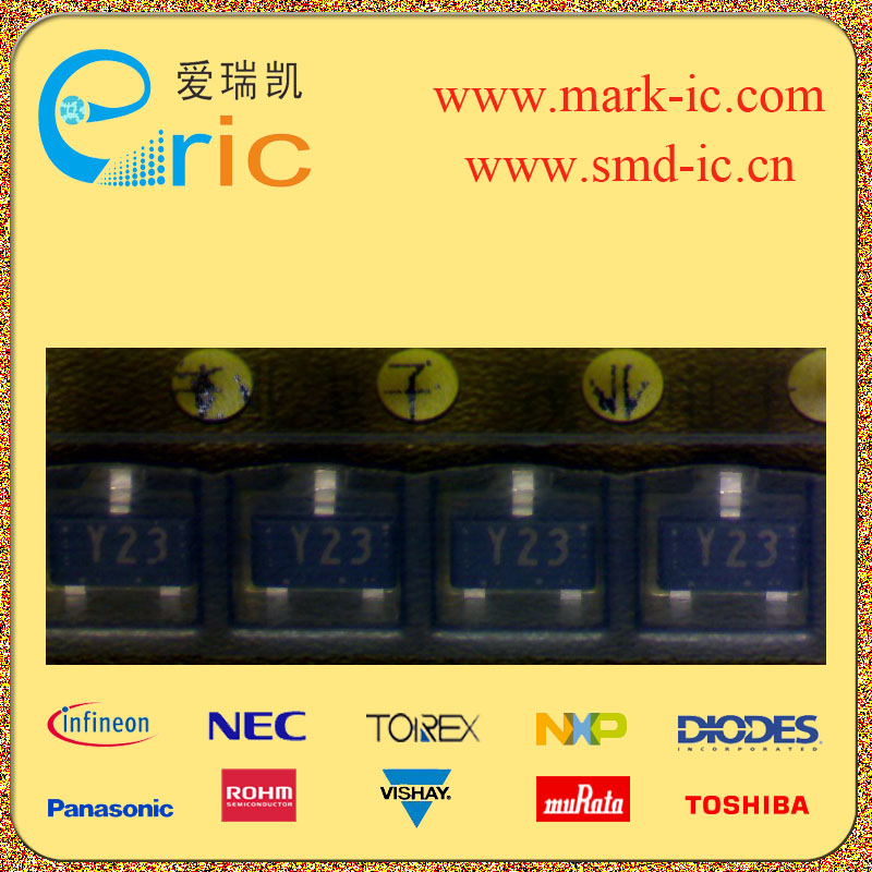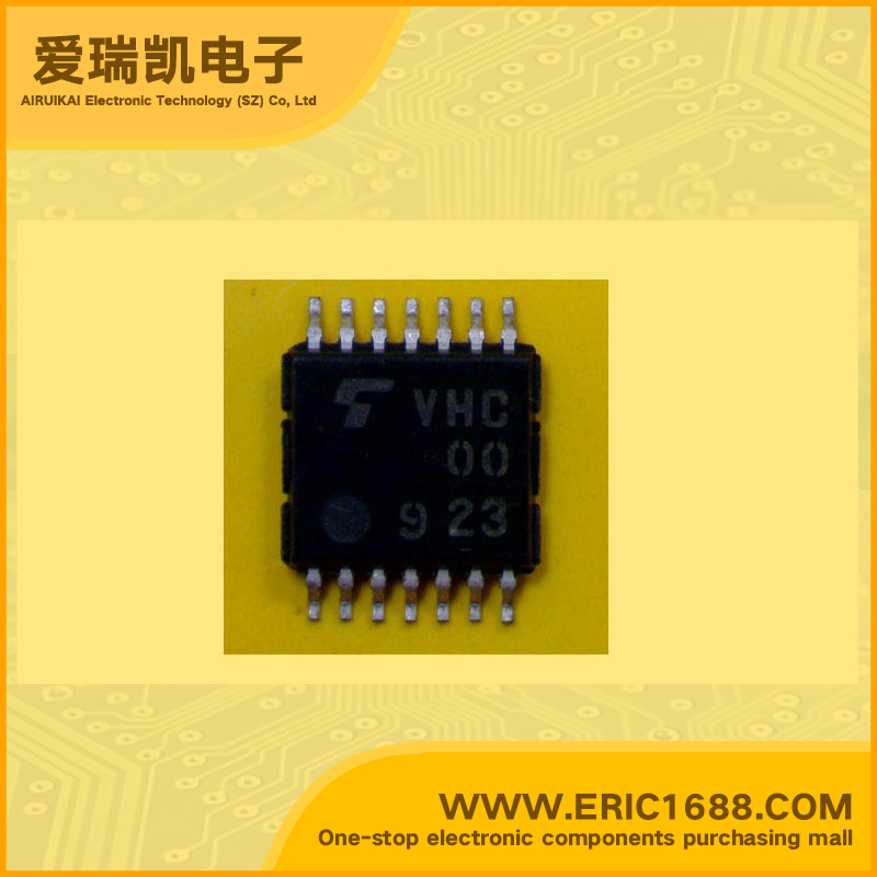
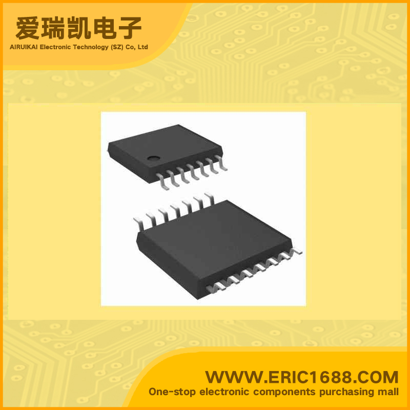
集成电路IC 与非门 TC74VHC00FT TSSOP14 marking/标记 VHC00
| 逻辑类型Logic Type | 与非门 NAND Gate |
| 电路数Number of Circuits | 4 |
| 输入数Number of Inputs | 2 |
| 电源电压VccVoltage - Supply | 2V~5.5V |
| 静态电流IqCurrent - Quiescent (Max) | 2µA |
| 输出高,低电平电流Current - Output High, Low | -8mA.8mA |
| 低逻辑电平Logic Level - Low | 0.5V |
| 高逻辑电平Logic Level - High | 1.5V |
| 传播延迟时间@Vcc,CLMax Propagation Delay @ V, Max CL | 7.5ns @ 4.5V~5.5V,50pF |
| Description & Applications | Quad 2-Input NAND Gate ;The TC74VHC00 is an advanced high speed CMOS 2-INPUT NAND GATE fabricated with silicon gate C2MOS technology. It achieves the high speed operation similar to equivalent Bipolar Schottky TTL while maintaining the CMOS low power dissipation. The internal circuit is composed of 3 stages including buffer output, which provide high noise immunity and stable output. An input protection circuit ensures that 0 to 5.5 V can be applied to the input pins without regard to the supply voltage. This device can be used to interface 5 V to 3 V systems and two supply systems such as battery back up. This circuit prevents device destruction due to mismatched supply and input voltages. • High speed: tpd = 3.7 ns (typ.) at VCC = 5 V • Low power dissipation: ICC = 2 μA (max) at Ta = 25°C • High noise immunity: VNIH = VNIL = 28% VCC (min) • Power down protection is provided on all inputs. • Balanced propagation delays: tpLH −∼ tpHL • Wide operating voltage range: VCC (opr) = 2 to 5.5 V • Low noise: VOLP = 0.8 V (max) • Pin and function compatible with 74ALS00 |
| 描述与应用 | 四路2输入与非门;TC74VHC00是一种先进的高速CMOS2输入 与非门制作与硅栅C2MOS技术。 它实现了高速操作类似等效 双极肖特基TTL同时保持了低功耗CMOS 耗散。 内部电路由3个阶段,包括缓冲区 输出,提供高抗干扰性和稳定的输出。 输入保护电路确保0到5.5 V可 没有考虑到电源电压施加到输入引脚。 该装置可用于接口5 V3 V系统和两个 如电池供电系统备份。该电路防止 由于设备破坏不匹配的电源和输入电压。 •高速:TPD =3.7纳秒(典型值),VCC= 5 V •低功耗:ICC= 2μA(最大值)在大= 25°C •高噪声,免疫力:VNIH= VNIL=28%VCC(分钟) •掉电保护是对所有投入。 •平衡传输时延:TPLH - TPHL •宽工作电压范围:VCC(OPR)=2至5.5 V •低噪声:VOLP=0.8 V(最大值) •引脚和功能兼容74ALS00 |
| 规格书PDF |