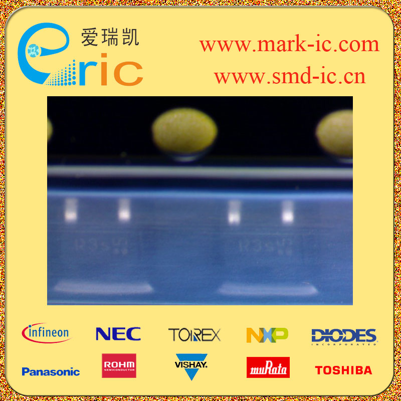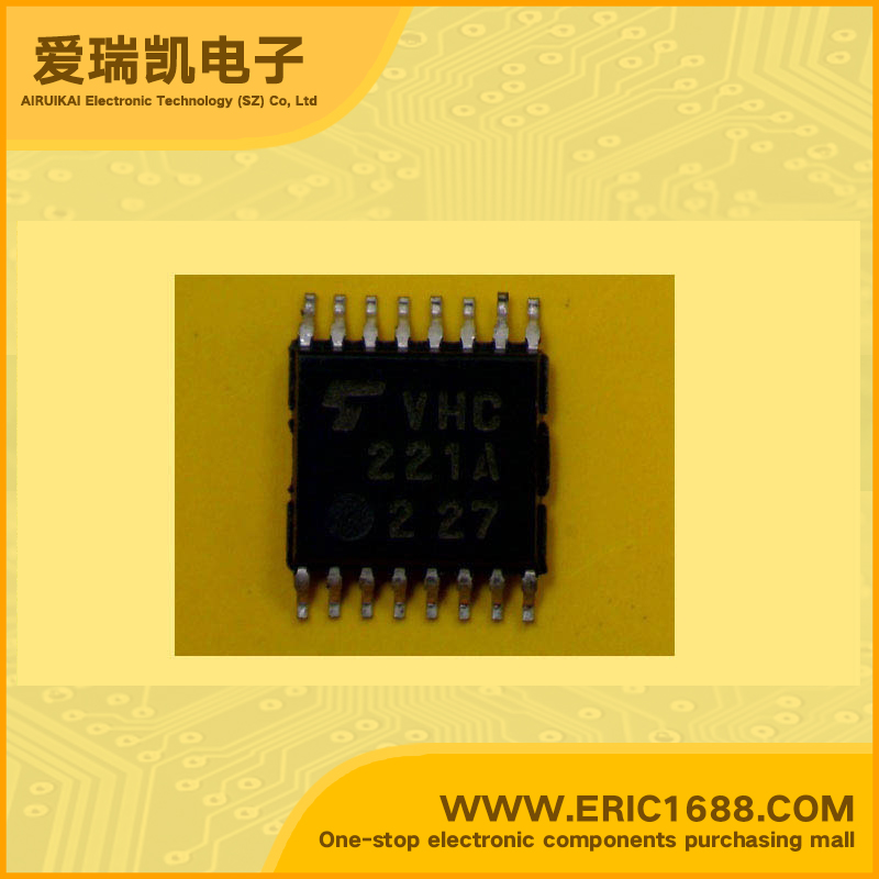
单稳态多谐振荡器 TC74VHC221A 16脚 marking/标记 VHC221A
| 逻辑类型Logic Type | 单稳态 Monostable |
| 电路数Number of Circuits | 1 |
| 输入数Number of Inputs | 无 No |
| 电源电压VccVoltage - Supply | 10.3ns |
| 静态电流IqCurrent - Quiescent (Max) | 20mA,20mA |
| 输出高,低电平电流Current - Output High, Low | 2 V ~ 5.5 V |
| 低逻辑电平Logic Level - Low | Dual Monostable Multivibrator Non-Retriggerble The TC74VHC123A/221A are high speed CMOS MONOSTABLE MULTIVIBRATOR fabricated with silicon gate C2MOS technology. There are two trigger inputs, A input (negative edge), and B input (positive edge). These inputs are valid for a slow rise/fall time signal (tr = tf = 1 s) as they are schmitt trigger inputs. This device may also be triggered by using CLR input (positive edge). After triggering, the output stays in a MONOSTABLE state for a time period determined by the external resistor and capacitor (RX, CX). A low level at the CLR input breaks this state. Limits for CX and RX are: External capacitor, CX: No limit External resistor, RX: VCC = 2.0 V more than 5 kΩ VCC ≥ 3.0 V more than 1 kΩ An input protection circuit ensures that 0 to 5.5 V can be applied to the input pins without regard to the supply voltage. This device can be used to interface 5 V to 3 V systems and two supply systems such as battery back up. This circuit prevents device destruction due to mismatched supply and input voltages. "Features • High speed: tpd = 8.1 ns (typ.) at VCC = 5 V • Low power dissipation Standby state: 4 μA (max) at Ta = 25°C Active state: 600 μA (max) at Ta = 25°C • High noise immunity: VNIH = VNIL = 28% VCC (min) • Power down protection is equipped with all inputs. • Balanced propagation delays: tpLH −∼ tpHL • Wide operating voltage range: VCC (opr) = 2 to 5.5 V • Pin and function compatible with 74HC123A/221A" |
| 高逻辑电平Logic Level - High | 双单稳多谐振荡器 TC74VHC123A/221A是高速CMOS 单稳态触发器制作与硅栅 C2MOS技术。 有两个触发输入,A输入(负沿),和B 输入(正面边缘)。这些投入是有效的一个缓慢的上升/下降(TR = TF=1秒)的时间信号,因为它们是施密特触发输入。这 设备也可以被触发通过使用CLR输入(上升沿)。 触发后,输出保持在一个单稳态 一段时间内由外部电阻器和电容器 (RX,CX)。 CLR输入在低水平打破这种状态。 CX和RX的限制是:外部电容,CX:不限制 外部电阻器,RX:VCC= 2.0 V超过5kΩ的VCC≥3.0 V超过1kΩ的 输入保护电路确保0到5.5 V可 没有考虑到电源电压施加到输入引脚。 该装置可用于接口5 V3 V系统和两个 如电池供电系统备份。该电路防止 由于设备破坏不匹配的电源和输入电压。 •高速:TPD = VCC= 5 V8.1纳秒(典型值) •低功耗 待机状态:4μA(最大值)在大= 25°C 活动状态:600μA(最大值)在大= 25°C •高噪声,免疫力:VNIH= VNIL=28%VCC(分钟) •掉电保护是所有输入配备。 •平衡传输时延:TPLH - TPHL •宽工作电压范围:VCC(OPR)=2至5.5 V •引脚和功能兼容74HC123A/221A“ |
| 传播延迟时间@Vcc,CLMax Propagation Delay @ V, Max CL | |
| Description & Applications | |
| 描述与应用 |
| 规格书PDF |