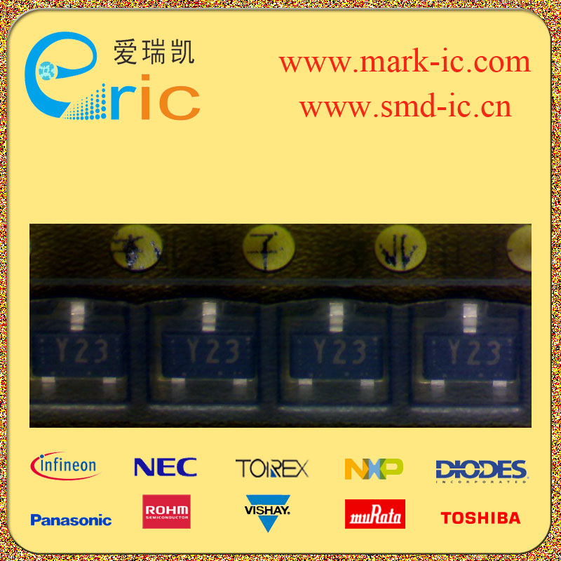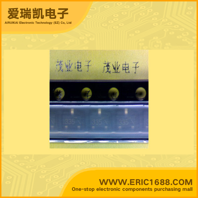
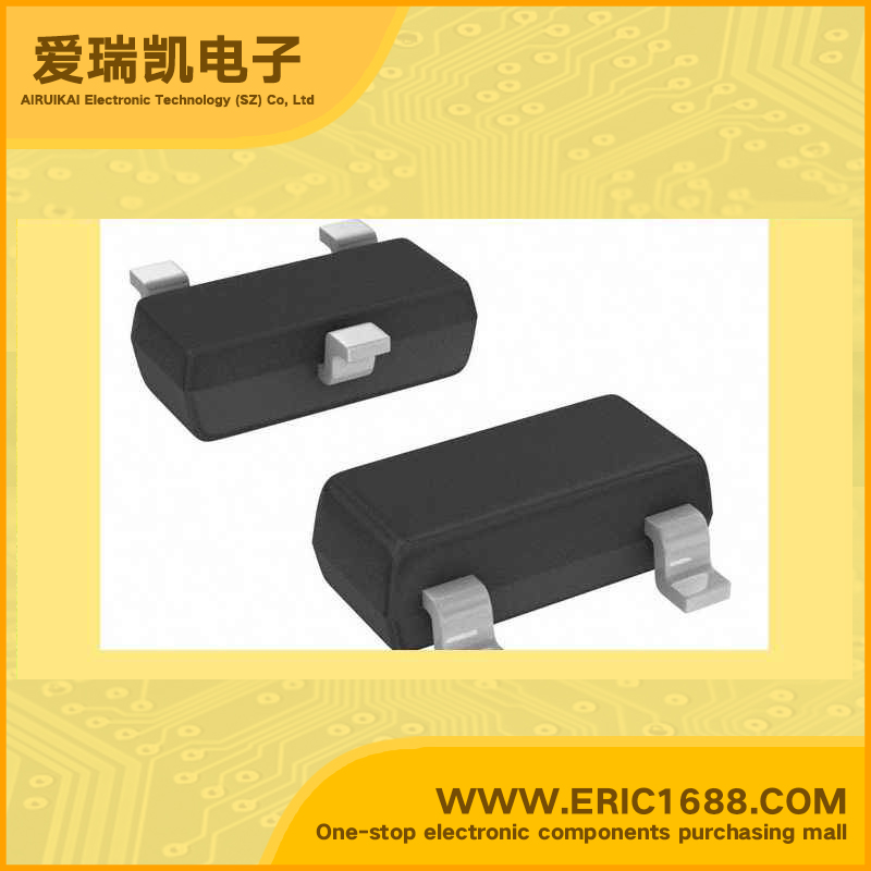
NDS335N N沟道MOSFET 20V 1.7A SOT-23/SC-59 marking/标记 335 高密度电池设计/良好导通电阻/最大DC电流能力
| 最大源漏极电压Vds Drain-Source Voltage | 20V |
| 最大栅源极电压Vgs(±) Gate-Source Voltage | 20V |
| 最大漏极电流Id Drain Current | 1.7A |
| 源漏极导通电阻ΩRds DΩ/Ohmain-SouΩ/Ohmce On-State Ω/Ohmesistance | 0.11Ω/Ohm @1.7A,4.5V |
| 开启电压Vgs(th) Gate-Source Threshold Voltage | 0.5-1V |
| 耗散功率Pd Power Dissipation | 500mW/0.5W |
| Description & Applications | N-Channel Logic Level Enhancement Mode Field Effect Transistor General Description These N -Channel logic level enhancement mode power field effect transistors are produced using Fairchild's proprietary, high cell density, DMOS technology. This very high density process is especially tailored to minimize on-state resistance. These devices are particularly suited for low voltage applications in notebook computers, portable phones, PCMCIA cards, and other battery powered circuits where fast switching, and low in-line power loss are needed in a very small outline surface mount package. Industry standard outline SOT-23 surface mount package using poprietary SuperSTM-3 design for superior thermal and electrical capabilities. High density cell design for extremely low RDS(ON) Exceptional on-resistance and maximum DC current capability. |
| 描述与应用 | N沟道逻辑电平增强模式场效应晶体管 概述 这些N沟道逻辑电平增强模式电源领域 场效应晶体管都采用飞兆半导体专有的生产, 高密度,DMOS技术。这非常高密度 过程特别是针对减少通态电阻。 这些器件特别适用于低电压 应用在笔记本电脑,便携式电话,PCMCIA 卡和其它电池供电的电路,开关速度快, 低线的功率损耗,需要在一个非常小外形 表面贴装封装。 行业标准外形SOT-23表面贴装封装 使用poprietary SuperSTM-3设计卓越的热 和电气性能。 高密度电池设计极低的RDS(ON) 卓越的导通电阻和最大DC电流能力 |
| 规格书PDF |