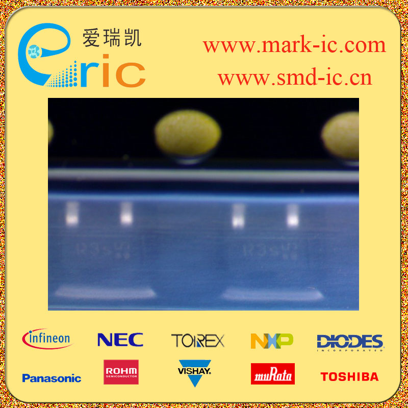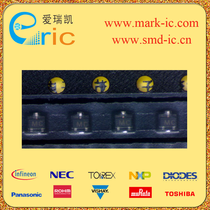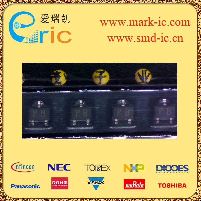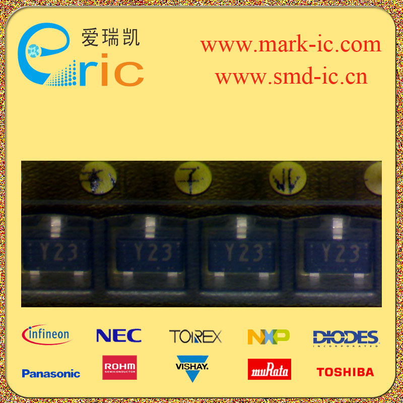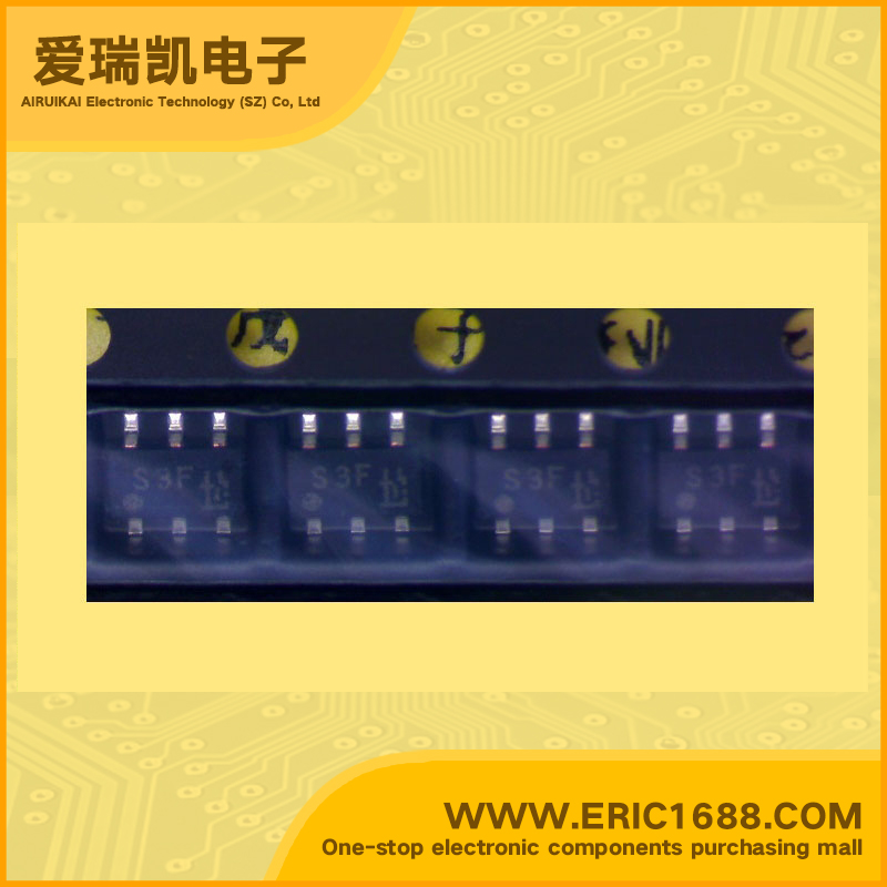
TPC6106 P沟道MOS场效应管 -40V -3.9A 75毫欧 SOT-163 marking/标记 S3F 便携式设备应用 低漏电流 低导通电阻
| 最大源漏极电压VdsDrain-Source Voltage | -40V |
| 最大栅源极电压Vgs(±)Gate-Source Voltage | 20V |
| 最大漏极电流IdDrain Current | -3.9A |
| 源漏极导通电阻RdsDrain-Source On-State Resistance | 75mΩ@ VGS = -10V, ID = -1.9A |
| 开启电压Vgs(th)Gate-Source Threshold Voltage | -0.85~-2.0V |
| 耗散功率PdPower Dissipation | 2.2W |
| Description & Applications | TOSHIBA Field Effect Transistor Silicon P Channel MOS Type (U-MOS II) Notebook PC Applications Portable Equipment Applications • Small footprint due to small and thin package • Low drain-source ON resistance: RDS (ON) = 58 mΩ (typ.) • High forward transfer admittance: |Yfs| = 5.5 S (typ.) • Low leakage current: IDSS = −10 μA (max) (VDS = −40 V) • Enhancement model: Vth = −0.8 to −2.0 V (VDS = −10 V, ID = −1 mA) |
| 描述与应用 | 东芝场效应晶体管硅P沟道MOS类型(U-MOS II) 笔记本电脑应用 便携式设备的应用 •由于占地面积小,小而薄的包装 •低漏源导通电阻RDS(ON)=58mΩ(典型值) •高正向转移导纳:| YFS|= 5.5 S(典型值) •低漏电流IDSS= -10μA(最大)(VDS=-40 V) •增强型号:Vth= -0.8到-2.0 V (VDS= -10 V,ID=-1毫安) |
| 规格书PDF |