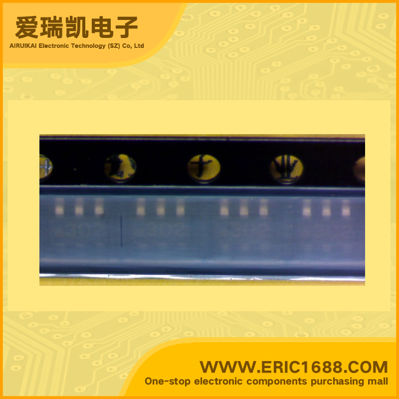
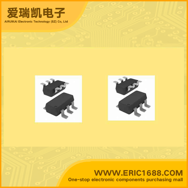
FDC6302P 复合场效应管 -25V -120mA/-0.12A SOT-163/SOT23-6/SSOT-6 marking/标记 302 双P沟道 数字FET
| 最大源漏极电压VdsDrain-Source Voltage | -25V |
| 最大栅源极电压Vgs(±)Gate-Source Voltage | -8V |
| 最大漏极电流IdDrain Current | -120mA/-0.12A |
| 源漏极导通电阻RdsDrain-Source On-State Resistance | 13Ω@ VGS = -2.7V, ID = -50mA |
| 开启电压Vgs(th)Gate-Source Threshold Voltage | -0.65~-1.5V |
| 耗散功率PdPower Dissipation | 900mW/0.9W |
| Description & Applications | Dual P-Channel , Digital FET General Description These dual P-Channel logic level enhancement mode field effect transistors are produced using Fairchild 's proprietary,high cell density, DMOS technology. This very high density process is especially tailored to minimize on-state resistance.This device has been designed especially for low voltage applications as a replacement for digital transistors. Since bias resistors are not required, these P-Channel FET's can replace several digital transistors, with a variety of bias resistors. Features Very low level gate drive requirements allowing direct operation in 3V circuits |
| 描述与应用 | 双P沟道,数字FET 概述 这些双P沟道逻辑电平增强模式场效应晶体管都采用飞兆半导体专有的,高细胞密度,DMOS技术。这非常高密度的过程特别是针对减少已经设计的状态resistance.This设备的,尤其是低电压应用程序替换为数字晶体管。由于偏置电阻器不是必需的,这些P沟道FET可以取代一些数字晶体管,偏置电阻器的各种。 特点 非常低的水平栅极驱动要求可直接操作3V电路 |
| 规格书PDF |