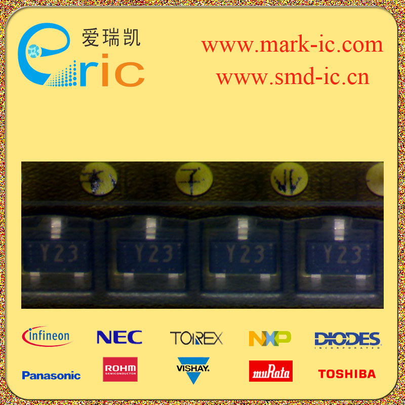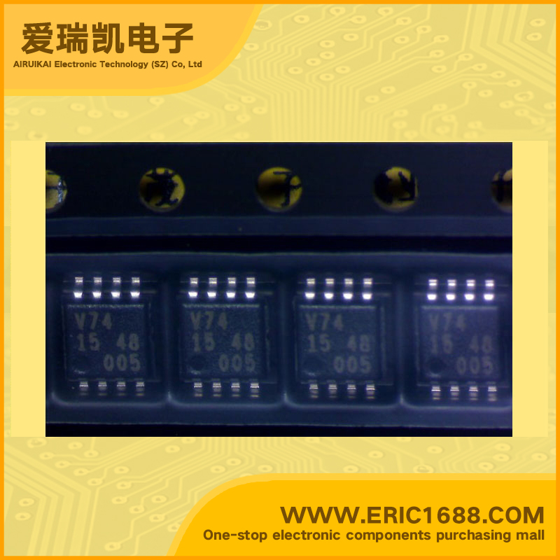
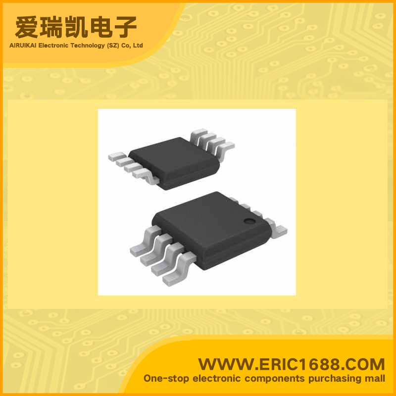
集成电路IC 上升沿触发器 74LVC2G74DP TSSOP8/SOT505-2 marking/标记 V74
| 逻辑类型Logic Type | 设置(预设)和复位 Set(Preset) and Reset |
| 电路数Number of Circuits | D型 D-Type |
| 输入数Number of Inputs | 差分 Differential |
| 电源电压VccVoltage - Supply | 1 |
| 静态电流IqCurrent - Quiescent (Max) | 1 |
| 输出高,低电平电流Current - Output High, Low | 200MHz |
| 低逻辑电平Logic Level - Low | 2.5ns |
| 高逻辑电平Logic Level - High | 正边沿 Positive Edge |
| 传播延迟时间@Vcc,CLMax Propagation Delay @ V, Max CL | 32mA,32mA |
| Description & Applications | 1.65 V ~ 5.5 V |
| 描述与应用 | Single D-type flip-flop; positive-edge trigger General description The 74LVC1G79 provides a single positive-edge triggered D-type flip-flop. Information on the data input is transferred to the Q-output on the LOW-to-HIGH transition of the clock pulse. The D-input must be stable one set-up time prior to the LOW to HIGH clock transition for predictable operation. Inputs can be driven from either 3.3 V or 5 V devices. This feature allows the use of this device in a mixed 3.3 V and 5 V environment. This device is fully specified for partial power-down applications using IOFF. The IOFF circuitry disables the output, preventing the damaging backflow current through the device when it is powered down. Wide supply voltage range from 1.65 V to 5.5 V High noise immunity Complies with JEDEC standard: JESD8-7 (1.65 V to 1.95 V) JESD8-5 (2.3 V to 2.7 V) JESD8B/JESD36 (2.7 V to 3.6 V) ESD protection: HBM JESD22-A114F exceeds 2000 V MM JESD22-A115-A exceeds 200 V 24 mA output drive (VCC = 3.0 V) CMOS low power consumption Latch-up performance exceeds 250 mA Direct interface with TTL levels Inputs accept voltages up to 5 V Multiple package options Specified from 40 C to +85 C and 40 C to +125 C. |
| 规格书PDF |