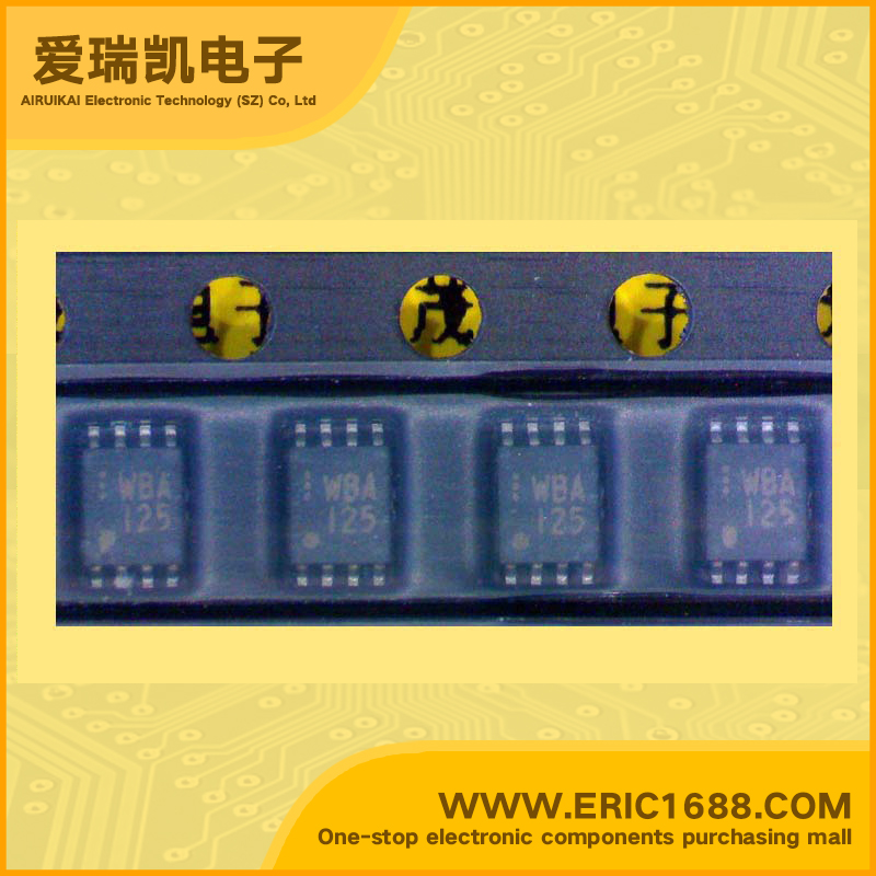
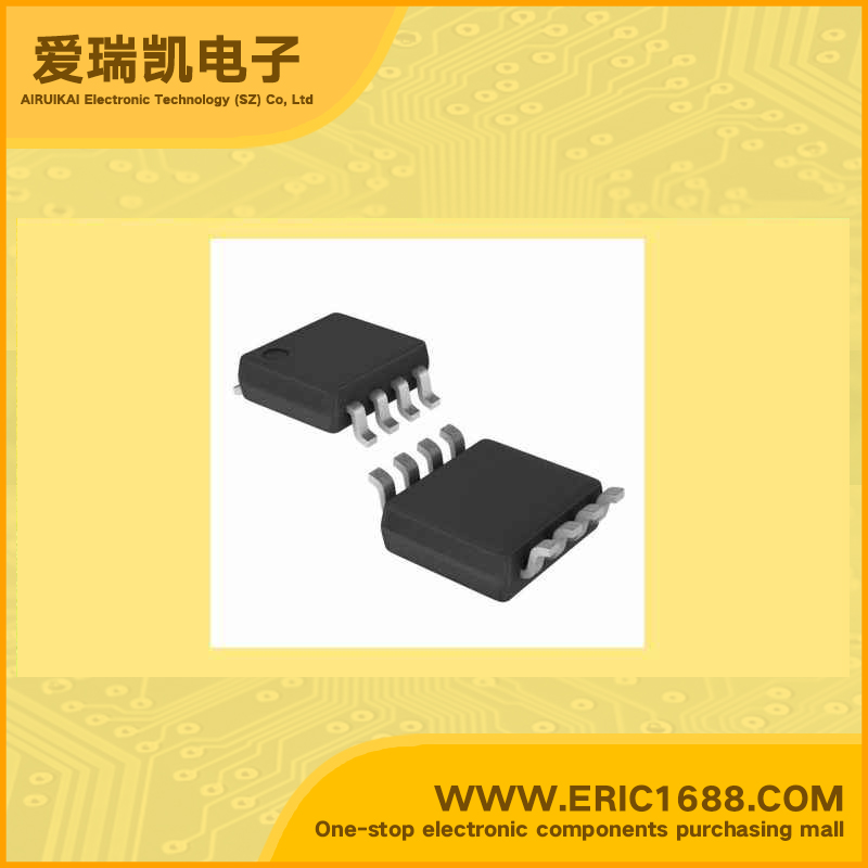
TC7WBD125AFK 解码器、多路复用器、信号开关 VFSOP8/US8 标记WBA125
| 逻辑类型Logic Type | 总线开关 Bus Switch |
| 电路数Number of Circuits | 1 x 1:1 |
| 输入数Number of Inputs | 2 |
| 电源电压VccVoltage - Supply | |
| 静态电流IqCurrent - Quiescent (Max) | 单电源 Single Supply |
| 输出高,低电平电流Current - Output High, Low | 4.5 V ~ 5.5 V |
| 低逻辑电平Logic Level - Low | The TC7WBD125AFK is a low on-resistance, high-speed CMOS 2-bit bus switch. This bus switch allows the connections or disconnections to be made with minimal propagation delay while maintaining Low power dissipation which is the feature of CMOS.When output enable (OE) is at low level, the switch is on; when at high level, the switch is off. The device is enable to realize the shift of signal level from 5 V to 3.3 V. All inputs are equipped with protector circuits to protect the device from static discharge. Operating voltage: VCC = 4.5~5.5 V High speed operation: tpd = 0.32 ns (max) Ultra-low on resistance: RON = 5 Ω (typ.) Electro-static discharge (ESD) performance: ±200 V or more (JEITA) ±2000 V or more (MIL) TTL level input (control input) Low Power Dissipation: Icc = 10 A (max.) Package: US8 |
| 高逻辑电平Logic Level - High | TC7WBD125AFK是一个低导通电阻,高速CMOS 2位总线开关。这个总线开关允许以最小的传播延迟连接或断开,同时保持CMOS低功耗的特点。当输出使能(OE)为低电平时,开关处于打开状态。为高电平时,开关处于关闭状态。该设备实现实现信号电平从5 V到3.3 V的移位。所有输入都配有保护电路的静电放电保护装置。 工作电压:VCC= 4.5〜5.5 V 高速运行:TPD =0.32 ns(最大) 超低电阻:RON= 5Ω(典型值) 静电放电(ESD)性能:±200 V或以上(JEITA)±2000 V以上(MIL) TTL电平输入(控制输入) 低功耗:ICC=10 A(最大) 包装:US8 |
| 传播延迟时间@Vcc,CLMax Propagation Delay @ V, Max CL | |
| Description & Applications | |
| 描述与应用 |
| 规格书PDF |