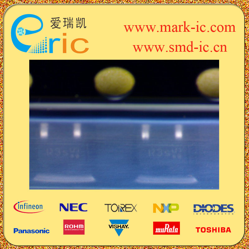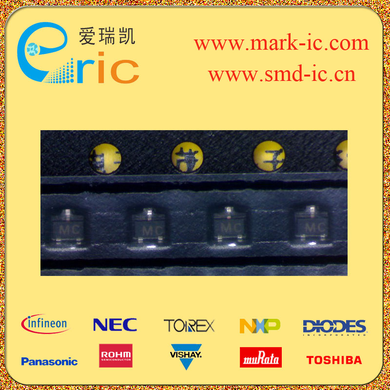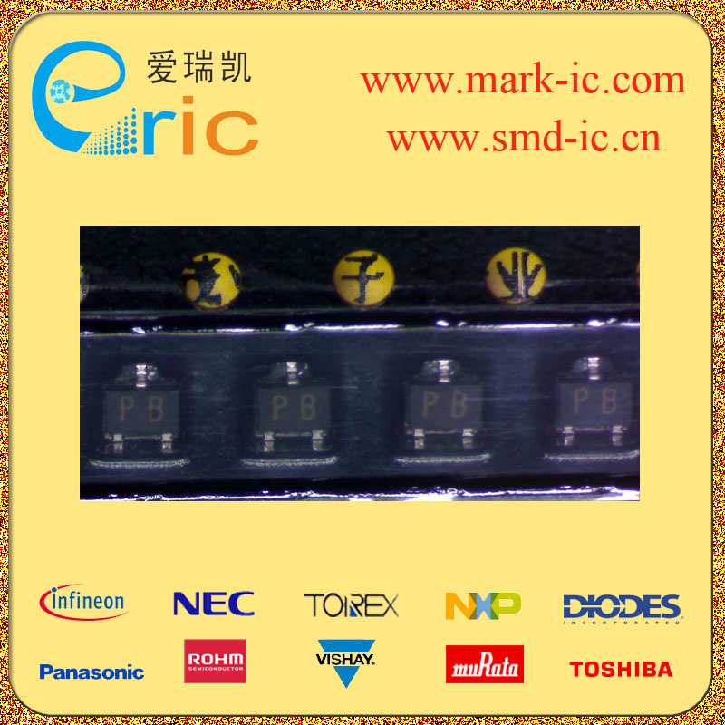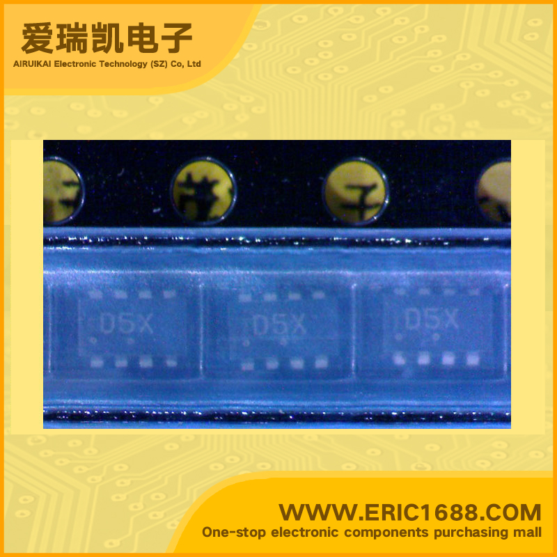
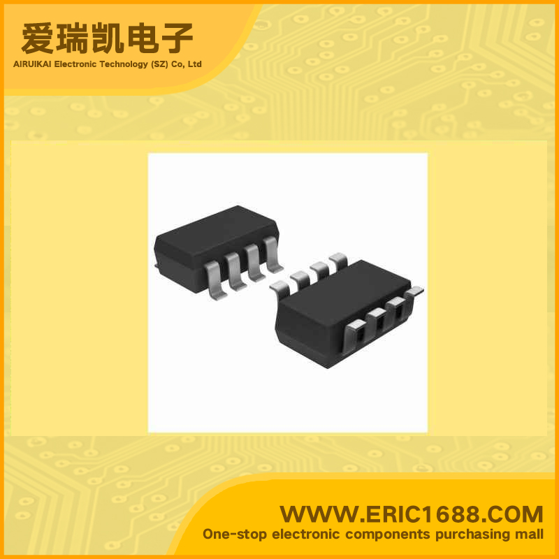
NTHD2102PT1G 复合场效应管 -8V -3.4A 1206-8/vs-8 marking/标记 D5X 功率MOSFET DC/DC转换
| 最大源漏极电压VdsDrain-Source Voltage | -8V |
| 最大栅源极电压Vgs(±)Gate-Source Voltage | -8V |
| 最大漏极电流IdDrain Current | -3.4A |
| 源漏极导通电阻RdsDrain-Source On-State Resistance | 160mΩ@ VGS = -1.8V, ID = -1A |
| 开启电压Vgs(th)Gate-Source Threshold Voltage | -0.45~-1.5V |
| 耗散功率PdPower Dissipation | 1.1W |
| Description & Applications | Power MOSFET Features • Offers an Ultra Low RDS(on) Solution in the ChipFET Package • Miniature ChipFET Package 40% Smaller Footprint than TSOP−6 making it an Ideal Device for Applications where Board Space is at a Premium • Low Profile (<1.1 mm) Allows it to Fit Easily into Extremely Thin Environments such as Portable Electronics • Designed to Provide Low RDS(on) at Gate Voltage as Low as 1.8 V, the Operating Voltage used in many Logic ICs in Portable Electronics • Simplifies Circuit Design since Additional Boost Circuits for Gate Voltages are not Required • Operated at Standard Logic Level Gate Drive, Facilitating Future Migration to Lower Levels using the same Basic Topology • Pb−Free Package is Available Applications • Optimized for Battery and Load Management Applications in Portable Equipment such as MP3 Players, Cell Phones, Digital Cameras, Personal Digital Assistant and other Portable Applications • Charge Control in Battery Chargers • Buck and Boost Converters |
| 描述与应用 | 功率MOSFET 特点 提供超低RDS(ON) 解决方案:在ChipFET包装 •微型ChipFET包装40%更小的体积比TSOP-6封装使其成为理想的装置应用电路板空间是一个溢价 •薄型(<1.1毫米)允许它能够轻松融入极薄环境,如便携式电子 •专为提供低RDS(ON)的栅极电压低至1.8 V,用于便携式电子产品在许多逻辑IC的工作电压 •简化电路设计,因为其他的栅极电压的升压电路不要求 •工作在标准逻辑电平栅极驱动,便于将来迁移到下级使用相同的基本拓扑结构 •无铅包装是可用 应用 •优化的便携式设备,如MP3播放器,手机,数码相机,个人数字助理和其它便携式应用的电池和负载管理应用程序 •电池充电器的充电控制 •降压与升压转换器 |
| 规格书PDF |