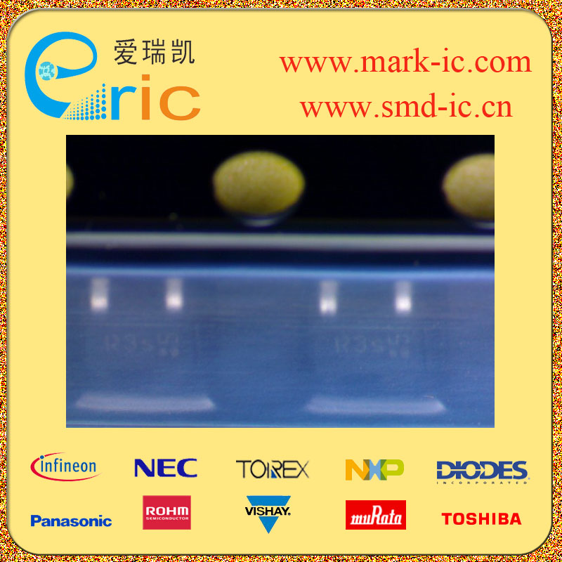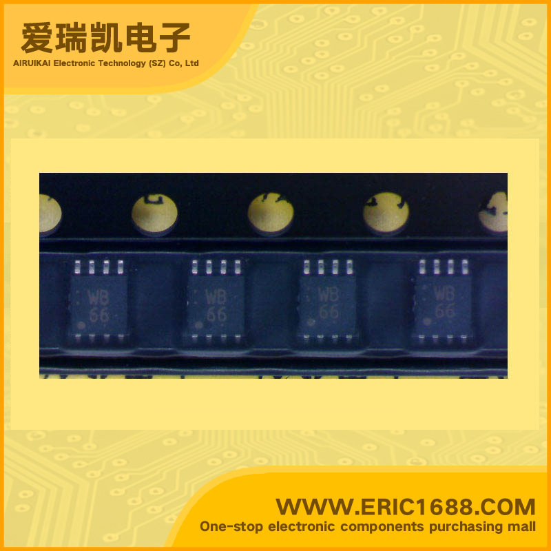
TC7WB66FK 解码器、多路复用器、信号开关 VFSOP8 标记7WB66
| 逻辑类型Logic Type | 总线开关 Bus Switch |
| 电路数Number of Circuits | |
| 输入数Number of Inputs | |
| 电源电压VccVoltage - Supply | |
| 静态电流IqCurrent - Quiescent (Max) | |
| 输出高,低电平电流Current - Output High, Low | 2V~5.5 V |
| 低逻辑电平Logic Level - Low | Dual Bus Switch CMOS digital integrated circuit silicon monolithic The TC7WB66FK is a low on-resistance, high-speed CMOS2-bit bus switch. This bus switch allows the connections or disconnections to be made with minimal propagation delay while maintaining Low power dissipation which is the feature of CMOS. When output enable (OE) is at High level, the switch is on; when at Low level, the switch is off. P-MOS and N-MOS channel block means the device is suitable for analog signal transmission. All inputs are equipped with protector circuits to protect the device from static discharge. High speed operation: tpd = 0.25 ns (max) Ultra-low on resistance: RON = 5 Ω (typ.) Electro-static discharge (ESD) performance: ±200 V or more (JEITA) ±2000 V or more (MIL) Power-down protection for inputs (control inputs only) |
| 高逻辑电平Logic Level - High | 双总线开关 CMOS数字集成电路硅单片 TC7WB66FK是一个低导通电阻,高速 CMOS2-bit总线开关。该总线开关允许连接或 以最小的传播延迟,而断开 保持低功耗的特点是 CMOS中。 当输出使能(OE)为高电平时,开关是开着的; 在低级别时,开关处于关闭状态。 P-MOS和N-MOS通道块的装置,该器件适合 为模拟信号的传输。 所有输入都配有保护电路,以保护 静电放电的设备。 静电放电(ESD)性能:±200 V或以上(JEITA) ±2000 V以上(MIL) 掉电保护的投入(仅控制输入) |
| 传播延迟时间@Vcc,CLMax Propagation Delay @ V, Max CL | |
| Description & Applications | |
| 描述与应用 |
| 规格书PDF |