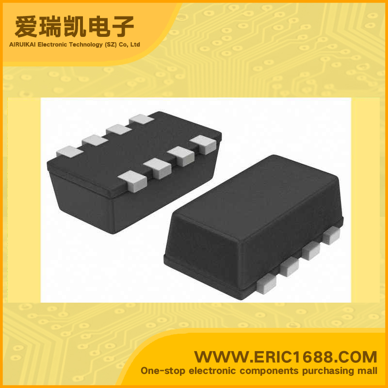
NTHS5441 P沟道MOS场效应管 -20V -3.9A 83毫欧 Vth:-0.6~-1.2V 1206-8 marking/标记 A3L 低导通电阻 高效率 便携式设备应用
| 最大源漏极电压VdsDrain-Source Voltage | -20V |
| 最大栅源极电压Vgs(±)Gate-Source Voltage | -12V |
| 最大漏极电流IdDrain Current | -3.9A |
| 源漏极导通电阻RdsDrain-Source On-State Resistance | 83mΩ@ VGS = -2.5V, ID = -3.1A |
| 开启电压Vgs(th)Gate-Source Threshold Voltage | -0.6~-1.2V |
| 耗散功率PdPower Dissipation | 1.3W |
| Description & Applications | Power MOSFET P-Channel Chip FET Features • Low RDS(on) • Higher Efficiency Extending Battery Life • Logic Level Gate Drive • Miniature ChipFET Surface Mount Package Applications • Power Management in Portable and Battery–Powered Products; i.e.,Cellular and Cordless Telephones and PCMCIA Cards |
| 描述与应用 | 功率MOSFET的P-通道芯片FET 特点 •低的RDS(on) •更高的效率延长电池寿命 •逻辑电平栅极驱动器 •微型ChipFET表面贴装封装 应用 •电源管理在便携式和电池供电的产品,也就是说,蜂窝电话和无绳电话和PCMCIA卡 |
| 规格书PDF |