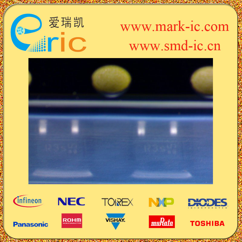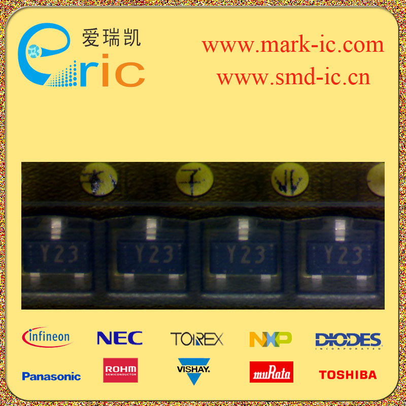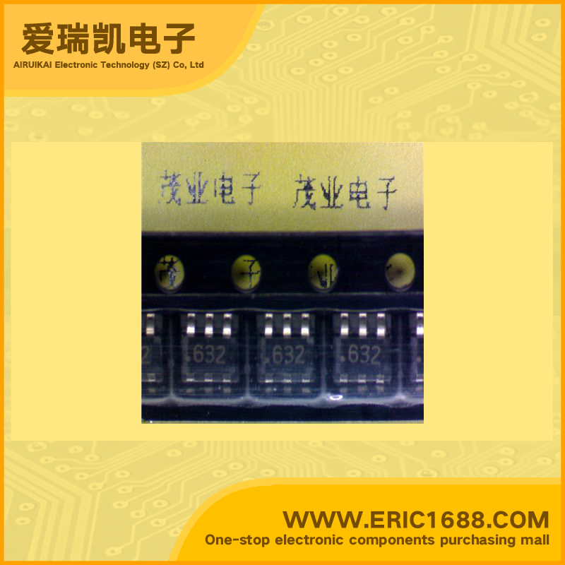
NDC632P P沟道MOS场效应管 -20V -2.7A 200毫欧 SOT-163 marking/标记 632
| 最大源漏极电压VdsDrain-Source Voltage | -20V |
| 最大栅源极电压Vgs(±)Gate-Source Voltage | -8V |
| 最大漏极电流IdDrain Current | -2.7A |
| 源漏极导通电阻RdsDrain-Source On-State Resistance | 200mΩ@ VGS = -2.7V, ID = -2.2A |
| 开启电压Vgs(th)Gate-Source Threshold Voltage | -0.4~-1V |
| 耗散功率PdPower Dissipation | 1.6W |
| Description & Applications | P-Channel Logic Level Enhancement Mode Field Effect Transistor Description These P-Channel logic level enhancement mode power field effect transistors are produced using Fairchild's proprietary, high cell density, DMOS technology. This very high density process is especially tailored to minimize on-state resistance. These devices are particularly suited for low voltage applications such as notebook computer power management and other battery powered circuits where fast high-side switching, and low in-line power loss are needed in a very small outline surface mount package. Feature Proprietary SuperSOT TM-6 package design using copper lead frame for superior thermal and electrical capabilities. High density cell design for extremely low RDS(ON). Exceptional on-resistance and maximum DC current capability. |
| 描述与应用 | P沟道逻辑电平增强模式场效应晶体管 描述 这些P沟道逻辑电平增强模式功率场效应晶体管都采用飞兆半导体专有的,高细胞密度,DMOS技术制作。这非常高密度的过程特别是针对减少通态电阻。 这些器件特别适用于低电压应用,如笔记本电脑电源管理和其他电池供电电路快速高侧开关和低线的功率损耗,需要在一个非常小外形表面贴装封装。 特点 专有SuperSOT TM-6包装设计采用铜引线框架的卓越的热性能和电气性能。高密度电池设计极低的RDS(ON)。 卓越的导通电阻和最大DC电流能力。 |
| 规格书PDF |