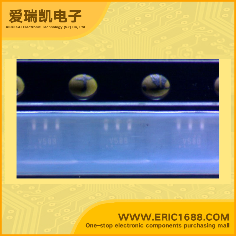
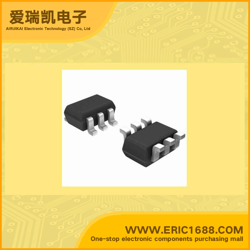
集成电路IC 可配置多功能GATE NC7SV58P6X SOT-363/SC70-6/MAA06A marking/标记 v58
| 逻辑类型Logic Type | 可配置多功能 Configurable Multiple Function |
| 电路数Number of Circuits | 1 |
| 输入数Number of Inputs | 2 |
| 电源电压VccVoltage - Supply | 是 Yes |
| 静态电流IqCurrent - Quiescent (Max) | 单端 Single-Ended |
| 输出高,低电平电流Current - Output High, Low | 24mA,24mA |
| 低逻辑电平Logic Level - Low | 0.9 V ~ 3.6 V |
| 高逻辑电平Logic Level - High | TinyLogic ULP Universal Configurable 2-Input Logic Gates General Description The NC7SP57 and the NC7SP58 are Universal Configurable 2-Input Logic Gates from Fairchild’s Ultra Low Power (ULP) Series of TinyLogic. Ideal for applications where battery life is critical, this product is designed for ultra low power consumption within the VCC operating range of 0.9V to 3.6V. Each device is capable of being configured for 1 of 5 unique 2-input logic functions. Any possible 2-input combinatorial logic function can be implemented as shown in the Function Selection Table. Device functionality is selected by how the device is wired at the board level. Figure 1 through Figure 10 illustrate how to connect the NC7SP57 and NC7SP58 respectively for the desired logic function. All inputs have been implemented with hysteresis. The internal circuit is composed of a minimum of inverter stages including the output buffer, to enable ultra low dynamic power. The NC7SP57 and NC7SP58, for lower drive requirements, are uniquely designed for optimized power and speed, and are fabricated with an advanced CMOS technology to achieve best in class operation while maintaining extremely low CMOS power dissipation. Features 0.9V to 3.6V VCC supply operation 3.6V overvoltage tolerant I/O’s at VCC from 0.9V to 3.6V Extremely High Speed tPD 2.5 ns typ for 2.7V to 3.6V VCC 3.1 ns typ for 2.3V to 2.7V VCC 4.0 ns typ for 1.65V to 1.95V VCC 6.0 ns typ for 1.4V to 1.6V VCC 8.0 ns typ for 1.1V to 1.3V VCC 23.0 ns typ for 0.9V VCC Power-Off high impedance inputs and outputs High Static Drive (IOH/IOL ±24 mA @ 3.00V VCC ±18 mA @ 2.30V VCC ±6 mA @ 1.65V VCC ±4 mA @ 1.4V VCC ±2 mA @ 1.1V VCC ±0.1 mA @ 0.9V VCC Uses patented Quiet Series noise/EMI reduction circuitry Ultra small MicroPak leadfree package Ultra low Dynamic Power |
| 传播延迟时间@Vcc,CLMax Propagation Delay @ V, Max CL | TinyLogicULP通用可配置2输入逻辑门 概述 NC7SP57和通用配置2输入逻辑门飞兆半导体的超低NC7SP58 功耗(ULP)系列TinyLogic。应用的理想选择 电池寿命是至关重要的,这款产品是专为 超低功耗内的VCC工作 0.9V至3.6V的范围内。每个器件都能够被配置为1-5个独特的2输入逻辑功能。 2输入的任何可能的组合逻辑函数可以是 实现功能选择表所示。 选择设备的功能是通过有线设备如何 在董事会层面。图1至图10说明了如何 连接的NC7SP57 NC7SP58分别为 所需的逻辑功能。所有的输入已实施滞后。 内部电路由逆变器的最小 阶段,包括输出缓冲器,以使超低 动态功耗。 该NC7SP57 NC7SP58,降低驱动器的要求,设计独特,优化的电源和速度,并制作了先进的CMOS技术,以达到最佳的类操作,同时保持极低的CMOS功耗。 0.9V至3.6V的VCC电源操作 3.6V过压容限I/ O的VCC从0.9V到3.6V 极高速的tPD 2.5纳秒典型为2.7V至3.6V的VCC 3.1纳秒典型为2.3V到2.7V VCC 4.0纳秒典型1.65V到1.95V VCC 6.0纳秒典型1.4V至1.6V VCC 8.0纳秒典型1.1V至1.3V VCC 23.0 ns(典型值)0.9V VCC 电源关闭高阻抗输入和输出 高静态驱动(IOH/ IOL ±24 mA@3.00V VCC ±18 mA@2.30V VCC ±6 mA@1.65V VCC ±4 mA@1.4V VCC ±2 mA@1.1V VCC ±0.1 mA@0.9V VCC 采用专利的静音系列噪声/ EMI减少 电路 超小型的MicroPak无铅封装 超低动态电源 |
| Description & Applications | |
| 描述与应用 |
| 规格书PDF |