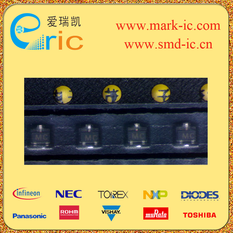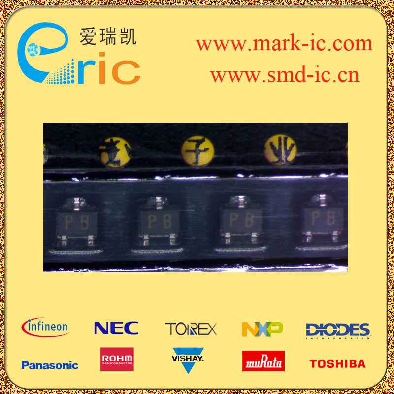

IRFR310BTM N沟道MOSFET 400V 1.7A TO-252/D-PAK marking/标记 门源齐纳ESD坚固
| 最大源漏极电压Vds Drain-Source Voltage | 400V |
| 最大栅源极电压Vgs(±) Gate-Source Voltage | 30V |
| 最大漏极电流Id Drain Current | 1.7A |
| 源漏极导通电阻ΩRds DΩ/Ohmain-SouΩ/Ohmce On-State Ω/Ohmesistance | 2.7Ω/OhmV @850mA,10V |
| 开启电压Vgs(th) Gate-Source Threshold Voltage | 2.0-4.0V |
| 耗散功率Pd Power Dissipation | 2.5W |
| Description & Applications | 400V N-Channel MOSFET General Description These N-Channel enhancement mode power field effect transistors are produced using Fairchild’s proprietary, planar, DMOS technology. This advanced technology has been especially tailored to minimize on-state resistance, provide superior switching performance, and withstand high energy pulse in the avalanche and commutation mode. These devices are well suited for high efficiency switch mode power supplies andelectronic lamp ballasts based on half bridge. • 1.7A, 400V, RDS(on) = 3.4Ω @VGS = 10 V • Low gate charge ( typical 7.7 nC) • Low Crss ( typical 6.0 pF) • Fast switching • 100% avalanche tested • Improved dv/dt capability |
| 描述与应用 | 400V N沟道MOSFET 概述 这些N沟道增强型功率场效应 晶体管都采用飞兆半导体专有的生产,平面,DMOS技术。 这种先进的技术,特别是针对已 最大限度地减少通态电阻,优越的开关性能,经受住了高能量脉冲 雪崩和减刑模式。这些器件非常 适用于高效率开关模式电源供应器和 电子镇流器基于半桥。 •低栅极电荷(典型7.7 nC) •低Crss(典型6.0 pF) •快速开关 •100%雪崩测试 •改进的dv / dt能力 |
| 规格书PDF |