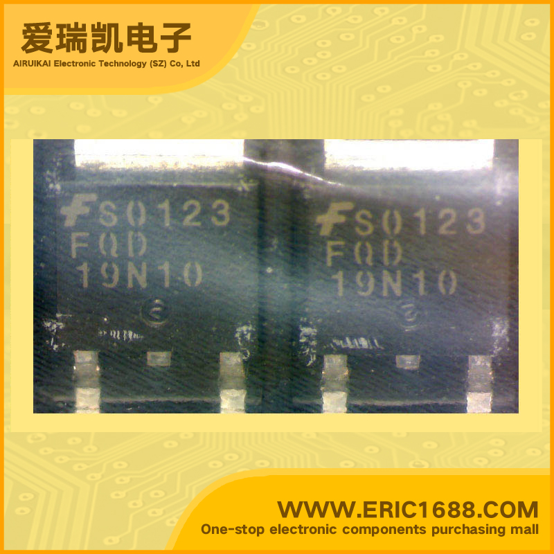
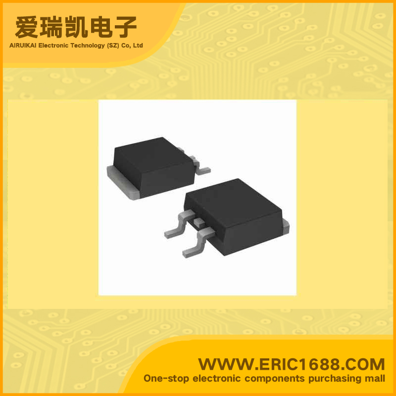
FQD19N10TM N沟道MOSFET 10V 15.6A TO-252/D-PAK marking/标记 FQD19N10 低栅极电荷/高速开关/极低的RDS
| 最大源漏极电压Vds Drain-Source Voltage | 10V |
| 最大栅源极电压Vgs(±) Gate-Source Voltage | 25V |
| 最大漏极电流Id Drain Current | 15.6A |
| 源漏极导通电阻ΩRds DΩ/Ohmain-SouΩ/Ohmce On-State Ω/Ohmesistance | 0.1Ω/Ohm 7.8A,10V |
| 开启电压Vgs(th) Gate-Source Threshold Voltage | 2.0-4.0V |
| 耗散功率Pd Power Dissipation | 2.5W |
| Description & Applications | N-Channel QFET ® MOSFET 200 V, 7.6 A, 360 mΩ Description This N-Channel enhancement mode power MOSFET is produced using Fairchild Semiconductor ®s proprietary planar stripe and DMOS technology. This advanced MOSFET technology has been especially tailored to reduce on-state resistance, and to provide superior switching performance and high avalanche energy strength. These devices are suitable for switched mode power supplies, active power factor correction (PFC), and electronic lamp ballasts. • 15.6A, 100V, RDS(on) = 0.1Ω @VGS = 10 V • Low gate charge ( typical 19 nC) • Low Crss ( typical 32 pF) • Fast switching • 100% avalanche tested • Improved dv/dt capability |
| 描述与应用 | QFET®N沟道MOSFET 200 V,7.6 A,360MΩ 描述 这N沟道增强模式功率MOSFET 产品采用飞兆半导体 ®专有 平面条形DMOS技术。这种先进的 MOSFET技术已特别针对 降低通态电阻,并提供卓越的 开关性能和高雪崩能量 实力。这些器件适用于开关模式 电源供应器,有源功率因数校正(PFC),以及电子镇流器。 •低栅极电荷(典型19nC) •低Crss(典型32 pF) •快速开关 •100%雪崩测试 •改进的dv / dt能力 |
| 规格书PDF |