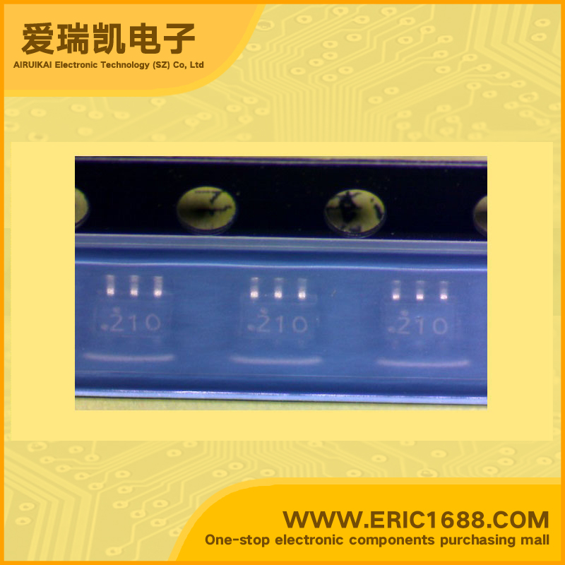
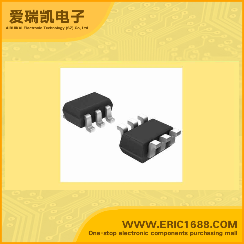
FDG6321C 复合场效应管 25V/-25V 500mA/-410mA SOT-363/SC70-6 marking/标记 21 双P沟道 数字FET
| 最大源漏极电压VdsDrain-Source Voltage | 25V/-25V |
| 最大栅源极电压Vgs(±)Gate-Source Voltage | 8V/8V |
| 最大漏极电流IdDrain Current | 500mA/-410mA |
| 源漏极导通电阻RdsDrain-Source On-State Resistance | 0.6Ω@ VGS =2.7V, ID =0.2A/1.5Ω@ VGS =-2.7V, ID =-0.25A |
| 开启电压Vgs(th)Gate-Source Threshold Voltage | 0.65~1.5V/-0.65~-1.5V |
| 耗散功率PdPower Dissipation | 300mW/0.3W |
| Description & Applications | Dual P-Channel, Digital FET General Description These dual N & P-Channel logic level enhancement mode field effect transistors are produced using Fairchild's proprietary, high cell density, DMOS technology. This very high density process is especially tailored to minimize on-state resistance. This device has been designed especially for low voltage applications as a replacement for bipolar digital transistors and small signal MOSFETS. Since bias resistors are not required, this dual digital FET can replace several different digital transistors, with different bias resistor values. Features Very small package outline SC70-6. Very low level gate drive requirements allowing direct operation in 3 V circuits |
| 描述与应用 | 双P沟道,数字FET 概述 这些双N&P沟道逻辑电平增强模式场效应晶体管都采用飞兆半导体专有的,高细胞密度,DMOS技术生产。这非常高密度的过程特别是针对减少通态电阻。该器件设计,尤其是作为一个替代双极数字晶体管和小信号MOSFET的低电压应用。由于偏置电阻器不是必需的,这双数字FET可以更换几个不同的数字晶体管,与不同的偏置电阻值。 特点 非常小的封装外形SC70-6。 非常低的水平栅极驱动要求可直接操作3 V电路 |
| 规格书PDF |